The race to build the world's most powerful AI chips isn't won solely at the transistor level anymore. Ask any semiconductor engineer where the real bottleneck lies, and they'll point you straight to the back end — specifically, to the packaging. At the centre of that conversation sits TSMC's CoWoS (Chip-on-Wafer-on-Substrate) platform: the advanced 2.5D packaging technology that has quietly become one of the most strategically important processes in the global technology supply chain.
From powering NVIDIA's Blackwell GPUs to enabling the next generation of hyperscaler AI accelerators, CoWoS is the invisible backbone of the AI boom. Here's a deep dive into why it matters, how it works, and what's coming next.
What Is CoWoS and Why Does It Matter for AI?
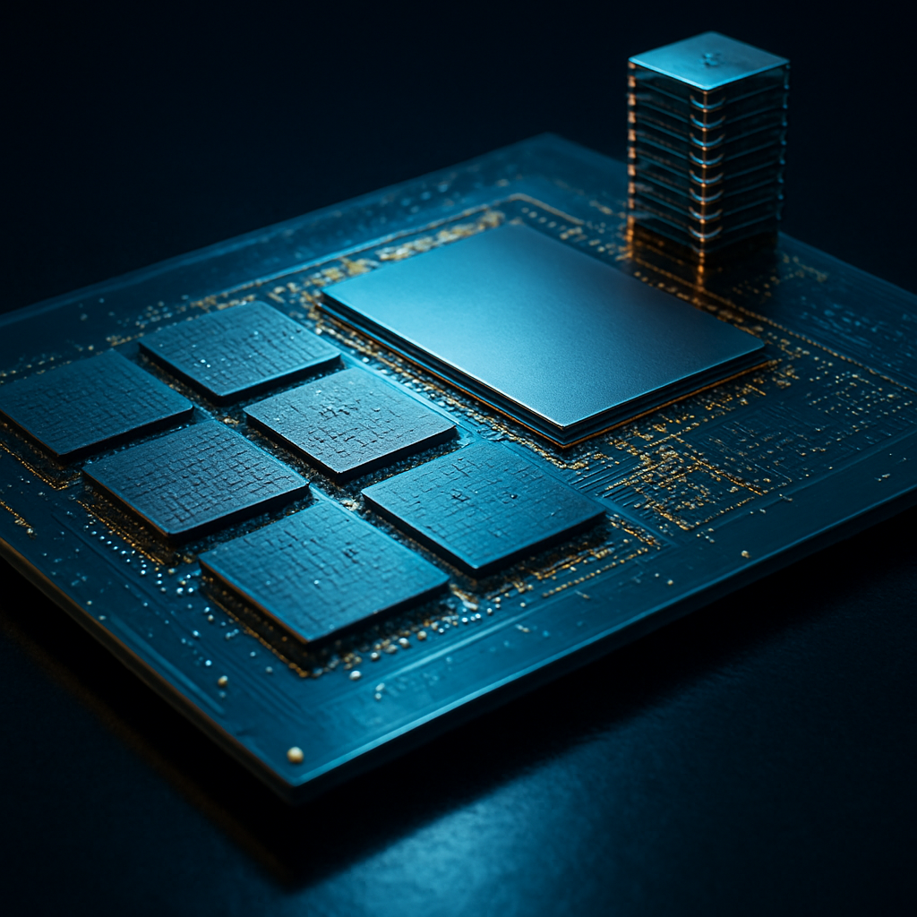
CoWoS (Chip-on-Wafer-on-Substrate) is TSMC's flagship 2.5D advanced packaging technology, introduced in 2012 to tackle the post-Moore's Law performance ceiling. It integrates multiple chiplets onto a silicon interposer, which is then connected to a package substrate.
The reason it's so critical for AI workloads comes down to memory bandwidth.
Instead of routing signals across long PCB traces, CoWoS enables near-die communication that's fast, power-efficient, and scalable — perfect for AI model training, large memory bandwidth applications, and high-performance computing (HPC).
CoWoS is the critical packaging process that enables High Bandwidth Memory (HBM) to sit next to GPUs and AI accelerators. Even if wafer supply increases, chips cannot be assembled without CoWoS capacity.
That dependency has made packaging — not just silicon fabrication — the defining constraint of the AI hardware era.
Breaking Down the CoWoS Family: S, L, and R
Not all CoWoS is created equal. TSMC has developed three distinct variants, each targeting different performance, size, and cost trade-offs.
CoWoS-S: The Original Workhorse
Since its 2012 debut, TSMC's CoWoS has become the gold standard for high-density AI and HPC integration, particularly when paired with HBM. CoWoS-S (silicon interposer) remains the workhorse for the most demanding designs.
CoWoS-S uses a silicon interposer with Through-Silicon Vias (TSVs), supports HBM integration, and is used in chips like NVIDIA's H100.
CoWoS-L: The Leap Beyond Reticle Limits
As AI chips like NVIDIA's Blackwell and the upcoming Rubin architectures grew in size and complexity, they began to exceed the "reticle limit" — the maximum size a single lithography step can print. To solve this, TSMC pivoted toward CoWoS-L (LSI Bridge), which uses Local Silicon Interconnect (LSI) bridges to "stitch" multiple chiplets together, allowing for packages several times larger than previous generations and accommodating more compute power and significantly more HBM.
CoWoS-L can stack up to 12 HBM3 devices at a lower cost than CoWoS-S and thus has the potential to become the mainstream CoWoS technology for future AI chips.
NVIDIA's CEO Jensen Huang has confirmed that the company's Blackwell architecture will transition from CoWoS-S to CoWoS-L advanced packaging technology.
CoWoS-R: The Cost-Focused Option
CoWoS-R (organic RDL interposer) offers cost trade-offs with reduced density
, making it suitable for workloads that don't require the extreme integration density of CoWoS-S or CoWoS-L. Together, the three variants give chip designers a tiered menu that balances performance, yield, and cost.
The Supply Crunch: A Bottleneck Shaping the AI Industry
If you've wondered why AI chip lead times stretch for months, CoWoS capacity is a major reason.
TSMC's CEO C.C. Wei acknowledged that packaging capacity is "very tight" and that TSMC is "working very hard to narrow the gap" between demand and supply.
CEOs from TSMC, SK Hynix, Micron, Intel, NVIDIA, and Samsung have all delivered the same message: demand for advanced nodes, advanced packaging, and high-bandwidth memory is rising much faster than capacity can be built. This is the clearest signal yet that AI's supply chain bottlenecks are not short-term "tightness" — they are structural limits that will shape pricing, lead times, and availability well into 2027.
TSMC is executing one of the most aggressive capacity expansions in semiconductor history specifically to address this AI chip packaging bottleneck. The company is scaling CoWoS production from approximately 35,000 wafers per month in late 2024 to a projected 130,000 wafers per month by the end of 2026 — nearly a 4x increase in under two years — and it is still not enough to fully satisfy demand.
To relieve pressure,
TSMC has even begun outsourcing some packaging steps to specialised third-party firms such as ASE and Amkor.
ASE Technology Holding continues to benefit from the spillover effect of CoWoS demand, with analysts assessing that ASE has the potential to secure orders from Broadcom, Nvidia, AMD, and Amazon for its front-end CoW process.
TSMC's Massive Infrastructure Push
To meet this demand, TSMC has been transforming its physical footprint at an unprecedented pace.
The AP6 facility in Zhunan, which became fully operational in late 2024, served as the initial catalyst for the capacity boost. The heavy lifting is now being handled by the AP8 facility in Tainan — a massive complex repurposed from a former display plant — and the burgeoning AP7 site in Chiayi.
AP7 is planned to house up to eight production buildings, specifically designed to handle the intricate "stitching" required for CoWoS-L and the integration of System-on-Integrated-Chips (SoIC), which stacks chips vertically before they are placed on a substrate.
Packaging is being treated like a globally strategic capacity, not a local afterthought. That has ramifications for every big tech company building AI hardware — because it means packaging capacity will increasingly be negotiated the way wafers are negotiated: multi-year commitments, priority queues, and ecosystem investments.
Driven by strong demand for cloud AI accelerators, global demand for CoWoS and similar packaging capacity may grow by 113% in 2025.
And
TSMC commands approximately 40% revenue share in advanced packaging for AI chips in 2025, particularly strong in 2.5D packaging solutions for AI/ML accelerators.
Why Wafer-Level Technology Keeps Winning Over Alternatives
Panel-level packaging has been touted as a potential successor to wafer-level tech, promising even larger package sizes. But TSMC is pushing back on that narrative — at least for now.
Although panel-level packaging technologies are set to enable much larger chip packages, they will not provide, at least initially, the same interconnection densities as today's wafer-level packaging technologies like CoWoS, according to Kevin Zhang, TSMC's Senior Vice President of Business Development.
The reason is deeply technical:
technologies like CoWoS use the same lithography, etching, deposition, and other tools that were previously used to make logic chips. By contrast, panel-level integration tools are considerably less advanced.
Meanwhile,
with Moore's Law slowing and advanced node costs climbing, 2.5D/3D packaging has become a primary driver of performance-per-watt and system-level efficiency, with TSMC's CoWoS platform setting the industry benchmark. CoWoS remains the gold standard for high-density AI/HPC accelerators that are tightly coupled with HBM.
The Road Ahead: TSMC's CoWoS Roadmap to 2029
TSMC's ambitions for CoWoS extend far beyond current production.
At the North American Technology Symposium 2026, TSMC revealed its updated CoWoS packaging roadmap with major enhancements.
The company is now producing 5.5-reticle size CoWoS and planning for even larger versions. A 14-reticle size CoWoS, capable of integrating approximately 10 large compute dies and 20 HBM stacks, is slated for production in 2028.
This will be followed by an expansion to beyond 14 reticles in 2029, complementing TSMC's 40-reticle size SoW-X System-on-Wafer technology also expected in 2029.
Combining silicon technology improvements and a larger CoWoS area, in 2029, TSMC will be able to cram 48x more transistors in a single package compared to 2024.
Such high integration is designed to meet the insatiable demand that AI accelerators have for both compute and memory bandwidth, and signals that packaging, not lithography, acts as a primary driver for semiconductor technologies.
Practical Tips for Chip Designers, Investors, and Tech Strategists
Understanding CoWoS isn't just academic — it has real implications for how you design products, allocate capital, and build supply chain strategies. Here's what to act on now:
- Secure packaging slots early.
CoWoS capacity remains extremely tight and is sold out through 2026.
If you're designing AI accelerators or custom ASICs, engage TSMC's packaging pipeline 18–24 months ahead of production timelines.
- Evaluate CoWoS-L for next-generation designs.
CoWoS-L enables extra-large silicon interposer areas — over 3,000 mm² — allowing for more chiplets and HBM stacks in a single package, enabling next-generation AI training systems that need terabytes of bandwidth and dense compute.
- Monitor OSAT partners for overflow capacity.
Companies like Amkor Technology and ASE Technology are no longer just "back-end" service providers; they are critical partners in the AI supply chain. By late 2025, OSATs have taken over the production of more mature advanced packaging variants, allowing foundries to focus their high-end capacity on the most complex 3D-IC projects.
- Watch the wafer-level packaging market.
The global wafer-level packaging market was estimated at USD 8.7 billion in 2025 and is expected to grow to USD 24.6 billion by 2035 at a CAGR of 11%.
For investors, this is a structural multi-year growth thesis.
- Plan around geopolitical concentration.
Taiwan-based companies dominate 76% of the advanced packaging market.
Supply chain diversification strategies should account for this concentration risk.
- Track TSMC's roadmap milestones. The jump to 14-reticle CoWoS in 2028 and beyond-14-reticle in 2029 will redefine what's possible in a single AI package — align your product roadmaps accordingly.
Conclusion: Packaging Is the New Process Node
The semiconductor industry spent decades laser-focused on shrinking transistors. Today, the competitive frontier has shifted.
The bottleneck for AI progress is no longer just the availability of advanced lithography machines, but the capacity of specialised packaging facilities. With AI giants like Nvidia and AMD pushing the boundaries of chip size, the ability to "stitch" multiple dies together with near-monolithic performance has become the defining competitive advantage.
TSMC's CoWoS platform — with its evolving S, L, and R variants, its aggressive capacity expansion, and its bold roadmap to 2029 — sits at the heart of that advantage. Whether you're a chip designer, a technology investor, or an enterprise strategist sourcing AI infrastructure, understanding CoWoS is no longer optional. It's foundational.
Want to stay ahead of the AI hardware curve? Subscribe to our newsletter for weekly deep dives into semiconductor strategy, supply chain intelligence, and the technologies reshaping the future of compute. The packaging revolution is just getting started — don't let it catch you off guard.